Table of contents
1. Meeting a LED cube 1.1. What is a LED cube? 1.2. Terminology 1.3. Breakdown 2. Electrical design 2.1. Scanning 2.2. Sketch 2.3. Prototypes 3. Mechanical design 3.1. Sketch 3.2. Steps 4. Software design 4.1. Steps 5. Cost
1. Meeting a LED cube
Somewhere in the summer of 2009, I entered the lobby of Fontys in Eindhoven. There I saw it for the first time: a LED cube. I'd never seen one before, and I immediately liked it. This cube was made by students, as a project, for Yacht. When I tried to explain the cube to my colleagues the next day, I suddenly had the brain wave to check YouTube for LED cubes. There are many, including the Fontys/Yacht one:
1.1. What is a LED cube?
When we talk about (computer) displays, we often talk about resolution. For example, a state of the art computer screen has 1920x1020 pixels each displaying over 16 million colors. The Nintendo DS handheld console has a screen of 256x192 pixels each displaying a quarter of a million colors. Smaller is possible. For example, the display below is a LED plane of about 7x20 pixels in one color (red).

A LED cube is special in one aspect: it is 3D. It consists of a series of ledplanes, standing as if in a line-up. A mechanical trick in LED cubes is that the LEDs are spaced quite far apart; this makes it ease to see-through each plane, so that all LEDs can be seen. As an illustration: the Fontys LED cube consists of 11 ledplanes, each being 11x11 pixels. The LEDs are single color (white) and they are spaced 5cm apart.
Some make relatively big LED cubes; I've seen 16x16x16. However, it should be noted that this takes 4096 LEDs. Not only a lot of work, but also quite expensive. Some use even multi color LEDs However, it should be noted that the wiring gets complex (see below).
1.2. Terminology
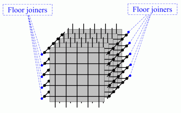
The picture below shows some terminology that I will use on this web page. A LED cube of order n consists of n x n x n LEDs. It is organized as n planes in a line-up. Their orientation gives them their nickname: walls. The first wall is typically referred to as the front wall, and the last wall is known as back wall. Each wall of a LED cube of order n is a led plane of n x n LEDs. See the picture below.
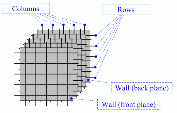
We see that each wall consists of n columns and n rows. At the intersection of the columns and rows, there is a LED. The notion of rows and walls is useful in mechanically assembling them. But, as we will see later, electrically, it makes more sense to talk about columns (n x n) being intersected by floors. The floors are the horizontal planes in the picture below.
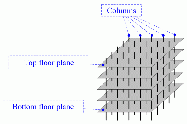
What this means is that once the walls are assembled, the rows at the same height are connected via a floor joiner; one on the left and one on the right. The result is a cube with n x n columns and n floors.
Suppose that we put the whole cube on a base. Furthermore, we add one wire from each floor to the base. Then, inside the base, there are n x n column wires plus n floor wires. In the next section, we explain how this suffices to drive the LEDs.
1.3. Breakdown
The production of a LED cube requires three disciplines: mechanical engineering (the base, the cube itself, a cover), electrical engineering (electrical circuit to drive the LEDs from a microcontroller) and software engineering (a program to drive the LEDs, showing nice animations). The next sections show the highlights of each of the disciplines.
2. Electrical design
2.1. Scanning
One important question when designing a LED cube is the electrical design, most notably how to drive the LEDs. It is unnecessarily complex to run two wires to each LED (this would mean 11x11x11x2 or 2662 wires for the Fontys cube). It is flexible (but not economical) to have one common wire for all LEDs plus a single driving wire per LED (this would mean 11x11x11+1 or 1332 wires for the Fontys cube). The Fontys LED cube features a third solution: scanning, which requires only (guessing) 11x11+11 or 132 wires.
2.2. Sketch
Since I had no experience with electrical design, I asked colleagues of mine (Oswald, Renķ, Klaas) for some clues (and reviews). These are the designs I made
- The first official sketch of the LED cube (electrical and even a mechanical) is still available as pdf or visio.
- The schematic and the layout pdf or visio
- To check whether the boards would fit in the base pdf or visio
2.3. Prototypes
LED cube version 1 Keil development board with an NXP LPC2148 processor. It runs a tiny program that switches on I/O pin P1.16 (top led on board), switches it off again, then switches on I/O pin P1.17 and switches it off again. These correspond to scan lines 0 and 1 on the breadboard. For each scan line, the columns 0 and 1 (corresponding to pins P1.20 and P1.21) are set to all for combinations. This is the first step towards a led cube.
LED cube version 1, testing the principle of scanning
LED cube version 2 In version 2 of my LED cube project, we see an NXP LPC2148 processor on a Keil development board. The development board is connected to a bread board with 5 columns (the final LED cube will have 25 columns - 5x5) and 5 rows (which will be the floors in the final LED cube) resulting in a network of 25 LEDs (the final LED cube will have 125 LEDs). The LCP2148 runs an interrupt service routine that puts a pattern on the columns, then switches on a row (floor). After a while the row (floor) is switched off, another pattern is put on the columns and the next row (floor) is switched on. After 5 rows (floor), the LPC wraps and starts with the first row (floor) again. So, 5 row (floor) patterns for 5 LED columns make up an image (in the final LED cube, this will be 5 floor patterns for 25 LED columns). At a much slower pace, one image is replaced by another (3 in total, forming the text JAN). A big disadvantage is the loss of intensity, now that each LED runs at 1/5th of its nominal intensity. From the top, the intensity is still ok, but from the side, the lack of brightness worries me.
LED cube version 2, one wall, real software
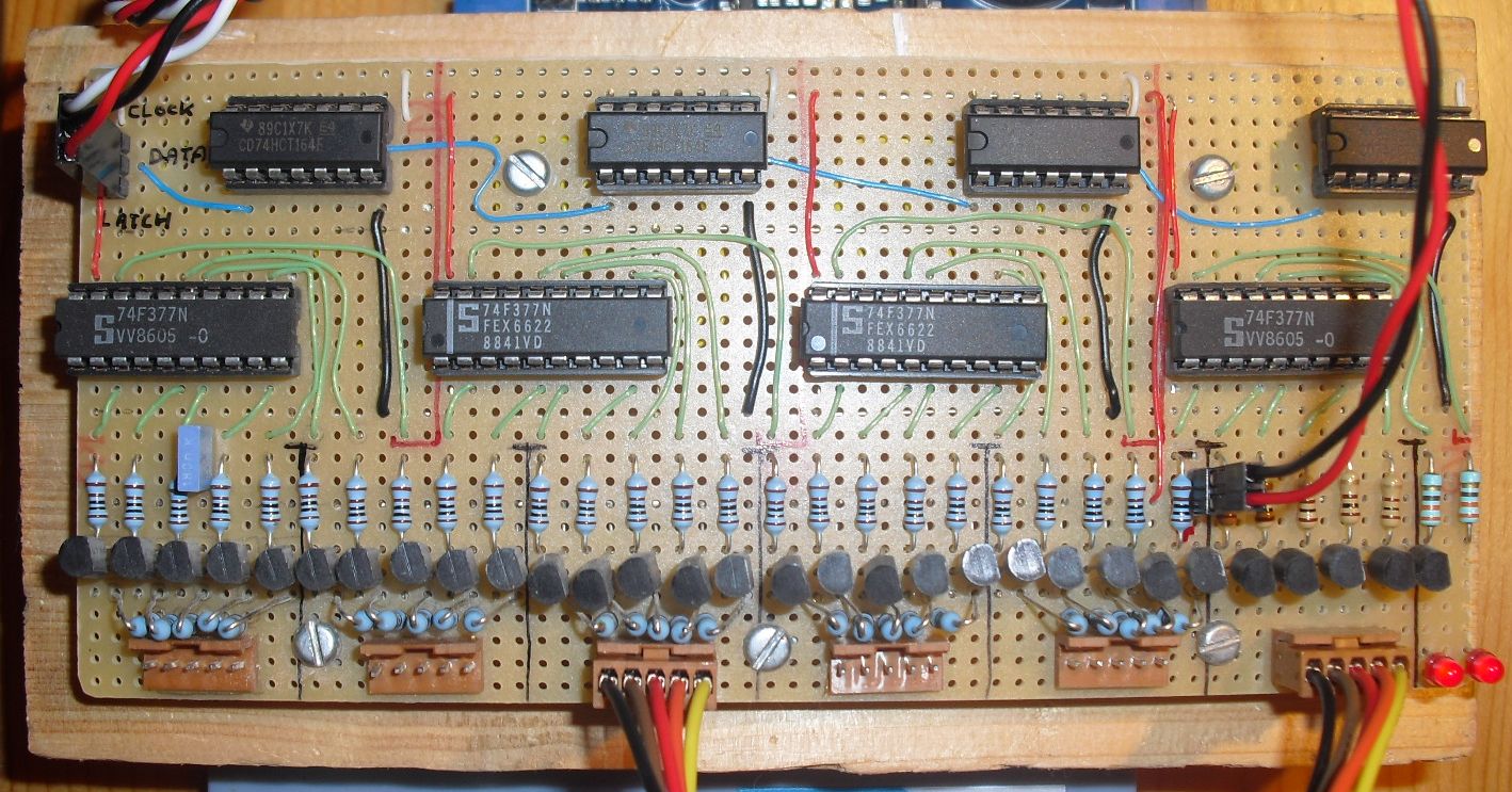
LED cube version 3 In version 3 of my LED cube project, we see an NXP LPC2148 processor on a Keil development board. The development board is connected to a bread board with 5 columns (the final LED cube will have 25 columns - 5x5) and 5 rows (which will be the floors in the final LED cube) resulting in a network of 25 LEDs (the final LED cube will have 125 LEDs). The connection between the development board and the breadboard has been improved greatly. Next to two wires for power (5V + GND from the USB), there are 3 wires for data: clock, data and latch. The clock and data line are connected to two cascaded (8-bit) "SIPO's" shift registers (1 line serial in and (2 times) 8 bit parallel out). The 16 output lines are wired through two octal D-flip-flops that are latched via a rising edge on the latch line.
LED cube version 3, prototyping the driver board
LED cube version 4 In version 4 of my LED cube project, we see an NXP LPC2148 processor on a Keil development board. The development board is connected to a driver board that has the capability to drive 25 columns and 5 floors. Only 5 columns and the 5 floors are connected to the breadboard of which only the right part is used: 5x5 LEDs. The connection between the keil board and the driver board is "thin": next to two wires for power (5V + GND), there are 3 wires to transfer the image for the LED cube: clock, data and latch. The clock and data line are connected to four cascaded (8-bit) SIPOs (1 line Serial In and 8 bit Parallel Out). The 32 output lines are wired through four octal D-flip-flops that are latched via a rising edge on the latch line. The latches control 5 times 5 transistors that drive the 25 columns of the LED cube; they control 5 transistors that drive the 5 floors of the LED cube; and there are two spare lines controlling to signal led (see top right of the driver board).
LED cube version 4, testing the driver board
LED cube version 5 In version 5 of my LED cube project, we no longer see the NXP LPC2148 processor on a Keil development board, nor the driver board. Both are now hidden in the base of a 5x5x5 LED cube. The animation is simple: all 5 wall show the same characters: JAN.GIJS.WOUTER.TEUN. Jan is the guy who helped me with this project: he did the mechanics of the LED cube. He's excellent, see his other work: http://www.youtube.com/profile?user=HEETGAS.
LED cube version 5, testing the LED cube
3. Mechanical design
3.1. Sketch
Jan Ridders (see his site) helped me with the mechanical part. First, he started making official, good looking, drawings.
- First version: wooden base with varnish, floor connectors assymetric staircased, column wires to the side of the LEDs, assymetric design
- Second version: wooden base black, floor connectors via extra columns on corners, column wires still to the side of the LEDs, symmetric design
- Third version: column wires behind the LEDs (bonus views)
- Proposal for a new base: front view and bottom view
- Fourth and final version: new base
- Addendum: inside the base pdf or visio
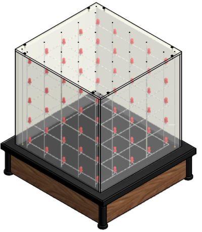
Excerpt from the technical drawing.
3.2. Steps
The first step entails creating the base: milling a slot for the perspex cover in the red (plastic) base plate, drilling holes for the 25 columns (and the 5 floor drivers) in the base plate, creating the four (plastic) feet (with slots for the wooden base sides), and sawing the four wooden base sides. The next step entails creating the perspex box: four sides and a top (with holes for the 25 columns and the 5 floor drivers), with some screw holes.

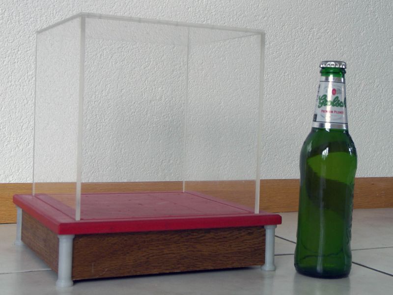
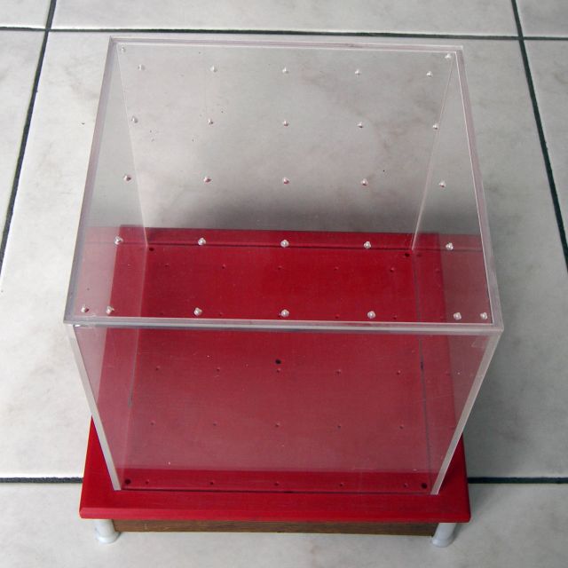
Creating the base and the perspex box
The third step entails soldering the LED rows (using a row mold to ensure uniform looks). In the next step, the LED rows are assembled into LED walls (again using a mold). Of course, LED wall should fit in the holes in the base plate and the perspex top.
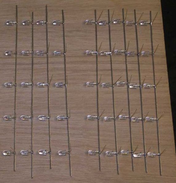
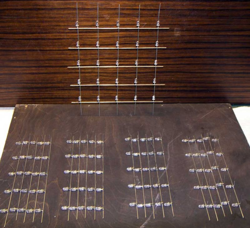
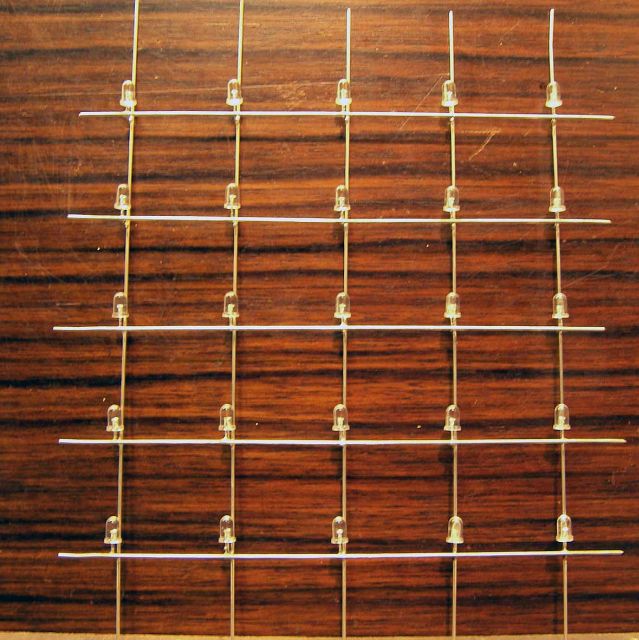
Creating the LED rows and LED walls
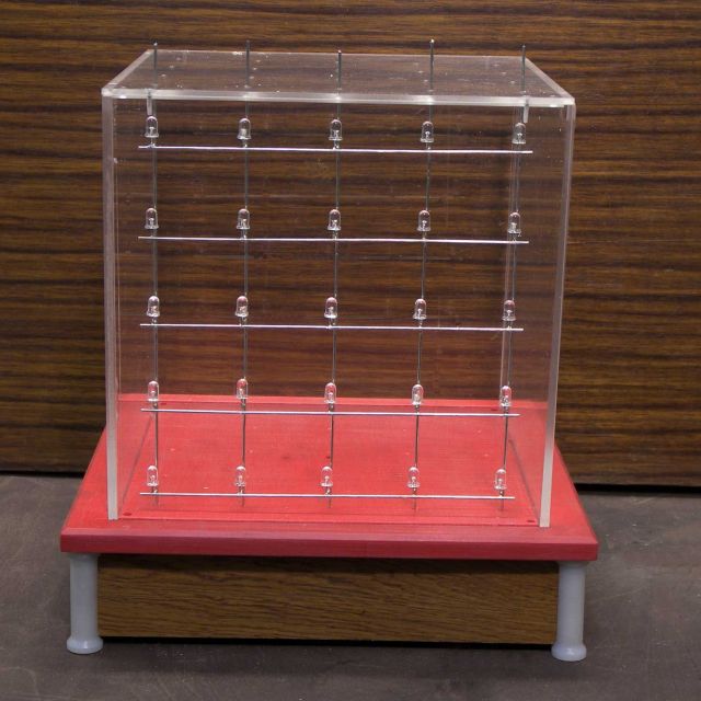
The fifth step entails mounting the walls in the base plate, and gently lowering the top plate (perspex). Note that the 25 holes on the base plate and top plate are self centering.
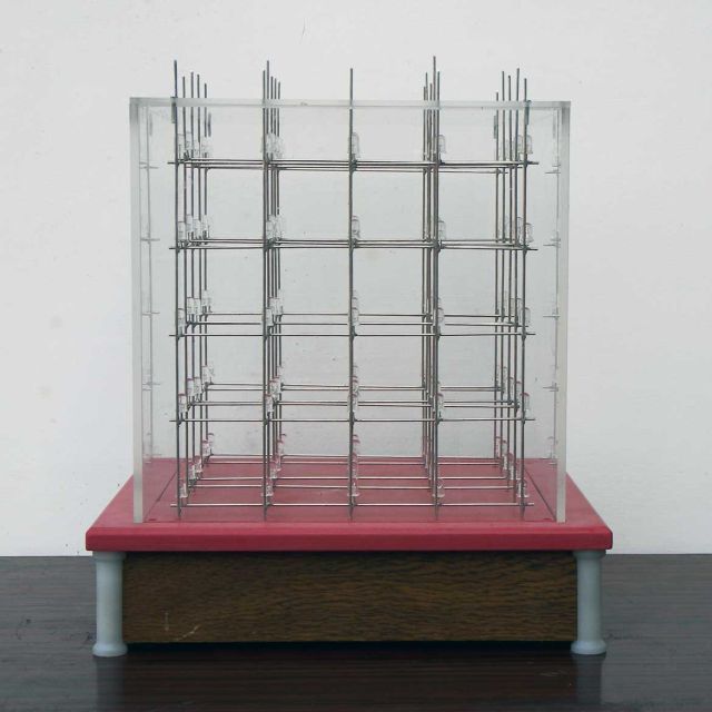

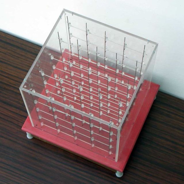
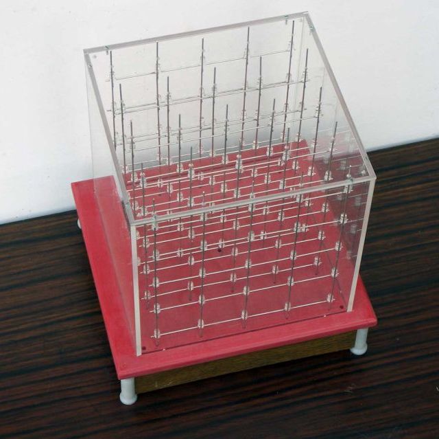
Assembling the walls in the box
Once the walls are positioned correctly, the 5 floor joiners on the left and the 5 floor joiners on the right are soldered, creating the complete cube. An until now unmentioned detail is that we have 5 extra "columns" (one on each corner and one in the center) to drive the floors. Also note that we have painted all wires white, and the base plate black.
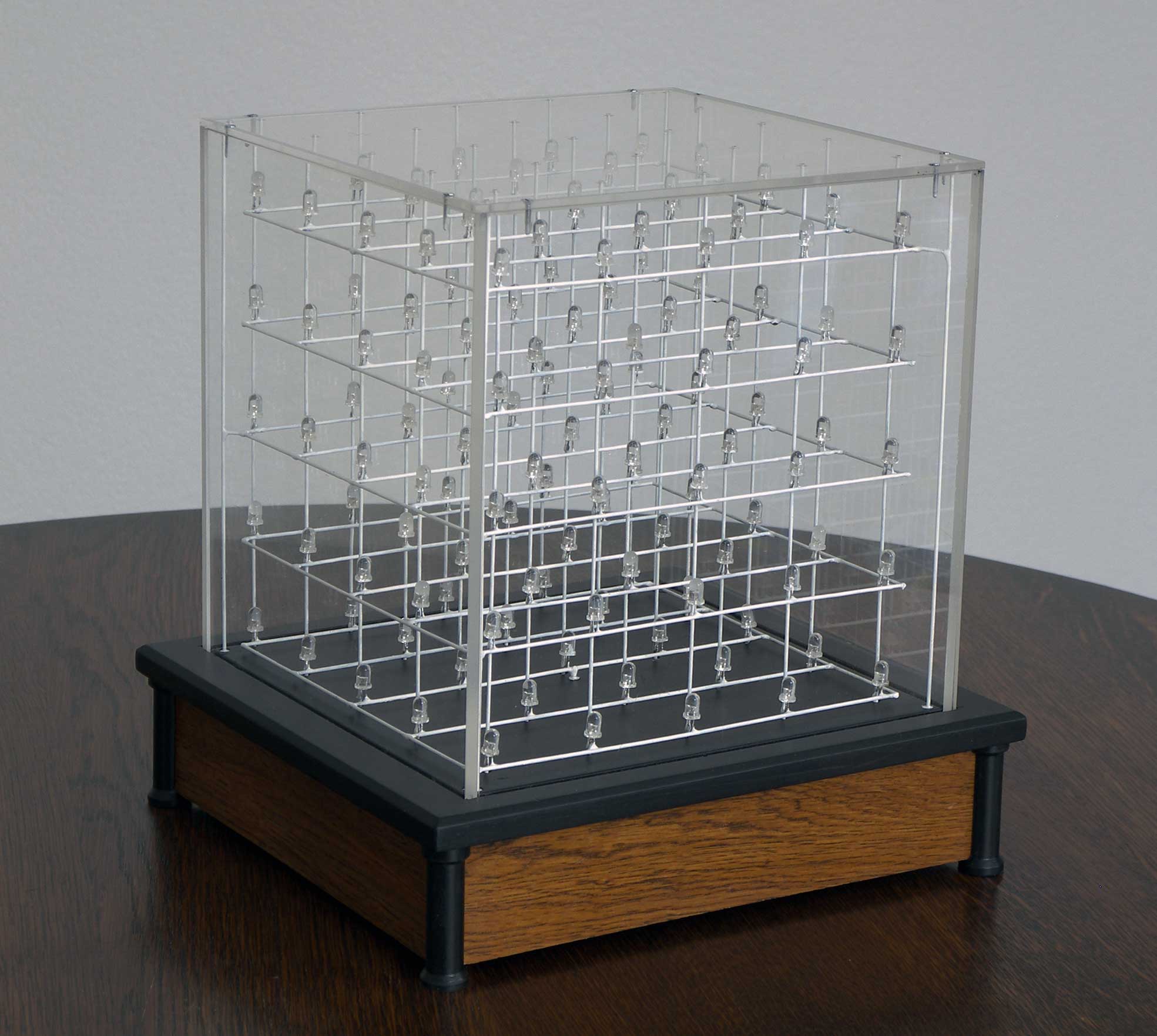
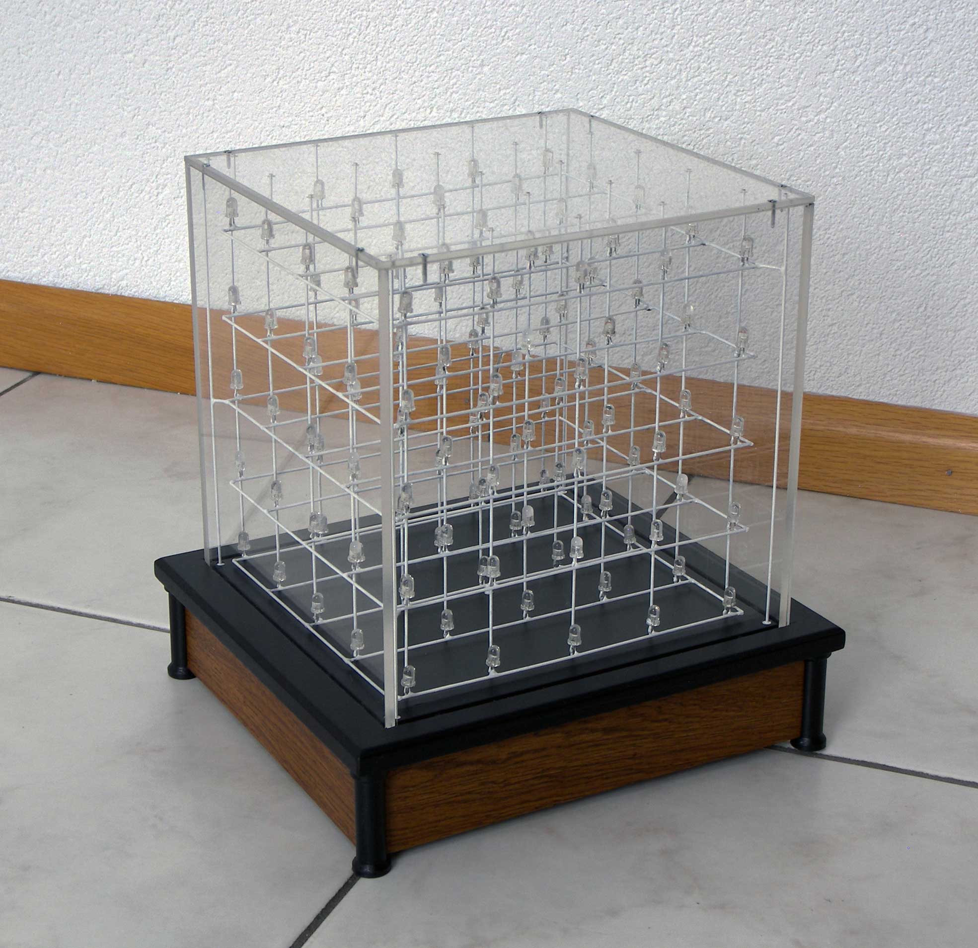
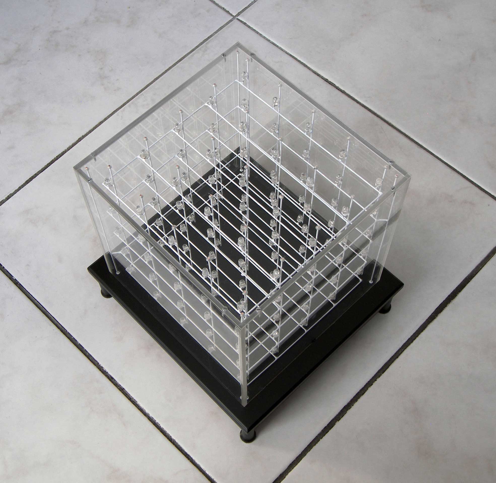
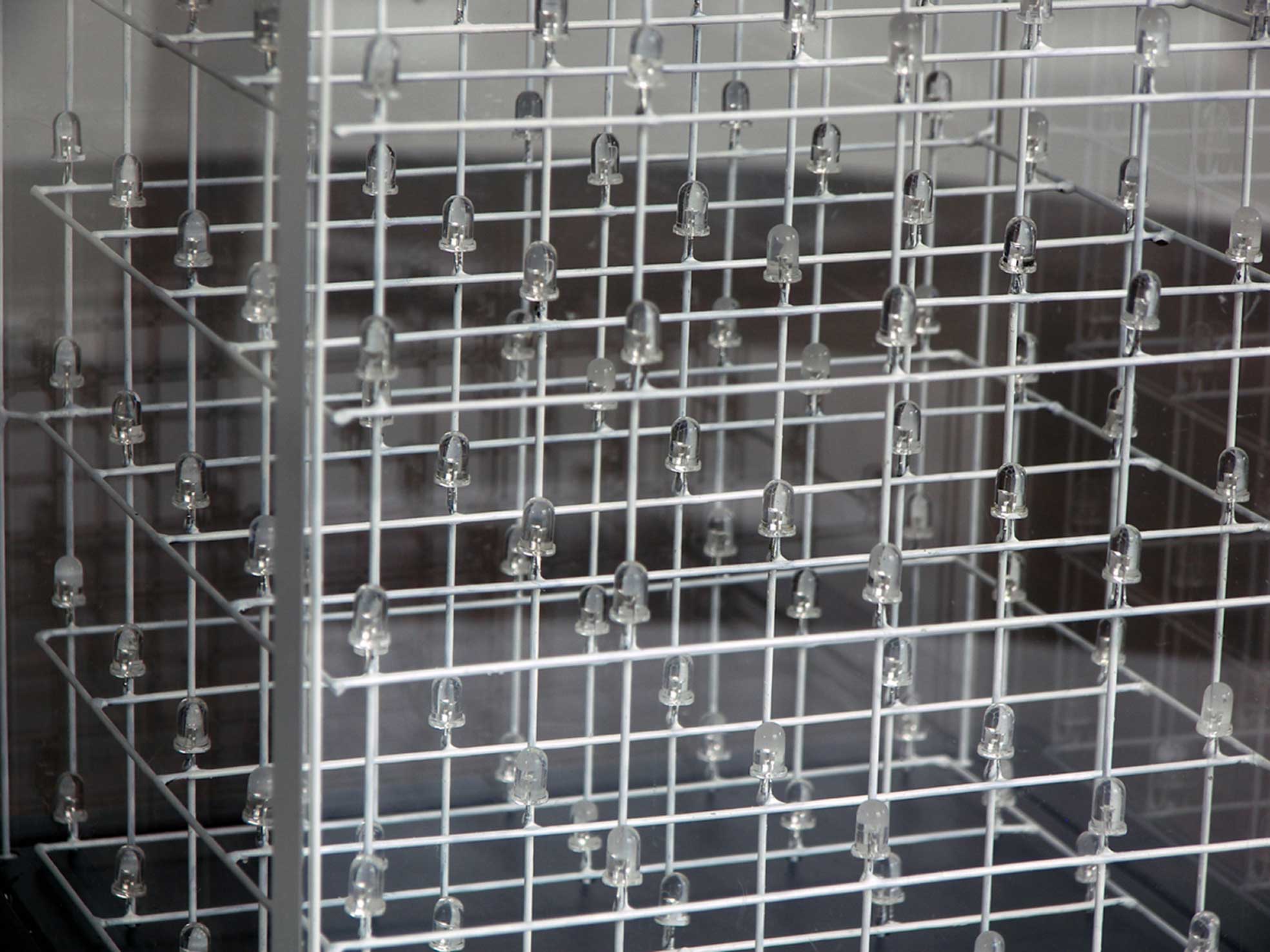
The final LED cube (assembled, painted)
4. Software design
4.1. Steps
5. cost
| item | description | quant | price | total |
|---|---|---|---|---|
| conrad 529593 | SOLDEER RASTERBORDEN FR2 | 1 | Ć 3.05 | Ć 3.05 |
| conrad 741230 | PRINTPLAAT STEEKVERB. 5POLIG | 6 | Ć 1.55 | Ć 9.30 |
| conrad 408042 | Metaalfilm weerstand 0,25W 100 Ohm 100st | 1 | Ć 2.17 | Ć 2.17 |
| conrad 408069 | Metaalfilm weerstand 0,25W 150 Ohm 100st | 1 | Ć 2.17 | Ć 2.17 |
| conrad 408166 | Metaalfilm weerstand 0,25W 1,0k Ohm 100st | 1 | Ć 2.17 | Ć 2.17 |
| conrad 189510 | IC-FITTING 14 POLIG | 4 | Ć 0.18 | Ć 0.72 |
| conrad 189545 | IC-FITTING 20 POLIG | 4 | Ć 0.27 | Ć 1.08 |
| conrad 151025 | High Speed CMOS 74 HCT 273 (Octale D-type flip-flop met clear) schematics use 74377 with chip enable i/o clear | 4 | Ć 0.33 | Ć 1.32 |
| conrad 150568 | High Speed CMOS 74 HCT 164 (Schuifregister SIPO 8-bit) | 4 | Ć 0.30 | Ć 1.20 |
| conrad 155918 | Transistor BC337/40 TO92 | 5 | Ć 0,18 | Ć 0.90 |
| conrad 155829 | Transistor BC327/40 TO92 | 25 | Ć 0,16 | Ć 4.00 |
| conrad 344388 | Hama USB laadapparaat "PICO" | 1 | Ć 15.99 | Ć 15.99 |
| conrad 180184 | LED 5mm superbright rood L53SRCDU | 125 | Ć 0,14 | Ć 17.50 |
| farnell 1741625 | ALPHA WIRE - 295 SV005 - WIRE, BUS BAR, 16AWG, 30.5M | 1 | Ć 17,74 | Ć 17,74 |
| stock | soldering tin | - | Ć - | Ć 3.00 |
| stock | wire | - | Ć - | Ć 3.00 |
| stock | perspex plate | 5 | Ć - | Ć 10.00 |
| stock | base plate | 1 | Ć - | Ć 10.00 |
| stock | base foot | 4 | Ć - | Ć 2.00 |
| stock | wooden base side | 4 | Ć - | Ć 2.00 |
| sparkfun 676 | Header board for LPC2148 We used Keil's MCB2140 Evaluation Board | 1 | Ć Ć28.19 | Ć Ć28.19 |
| total | Ć 137.50 |
